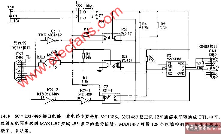
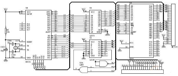
CAN bus communication hardware schematic diagram (using TJA1050T CAN bus driver)
F040 built-in CAN bus protocol controller, as long as the external bus driver chips and appropriate anti-jamming circuit can easily build a CAN bus intelligent control node. This design uses PHILIP company TJA1050T CAN bus driver.
CAN bus communication hardware schematic diagram shown in Figure 3.

F040 figure of CAN signal reception pin RX and TX pins are not sent directly connected to TJA1050T RXD and TXD end, but through the high-speed optocoupler connection 6N137, that the purpose is to achieve electrical CAN bus each node isolation. In order to achieve complete electrical isolation in the true sense, the optocoupler section VA and VB must be isolated by the DC-DC switching power supply module or modules with multiple isolated outputs. To prevent over-current shock, TJA1050T the CANH and CANL pins each connected to the bus via a resistor of a 5Ω. And between CANH and CANL feet and capacitors in parallel two 30P for the bus frequency interference filter. The lightning D1 and D2 may play a protective role in the occurrence of transient interference.
TJA1050T F040 8-pin connector to a port for mode selection, TJA1050T There are two operating modes for selection, high-speed mode and silent mode. TJA1050T to work in high-speed mode, and in silent mode, TJA1050T the transmitter is disabled, perform listen function can be used to prevent the network due to the CAN controller out of control and cause obstruction.


