Power, clock and reset circuit diagram (Altera FPGA development board) as shown:
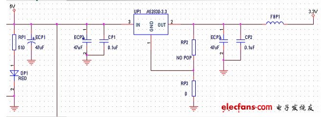
Figure power, clock and reset circuit diagram (Altera FPGA development board) Figure Clock Circuit (Altera FPGA development board) Figure Reset Circuit (Altera FPGA development board)
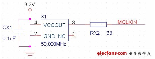
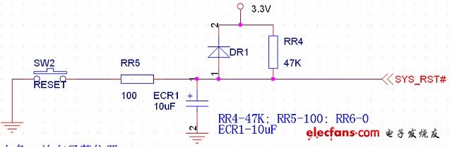
Figure power, clock and reset circuit diagram (Altera FPGA development board) Figure Clock Circuit (Altera FPGA development board) Figure Reset Circuit (Altera FPGA development board)
No comments:
Post a Comment
Please comment