Monday, August 18, 2014

CAN bus communication hardware schematic diagram (using TJA1050T CAN bus driver


CAN bus communication hardware schematic diagram (using TJA1050T CAN bus driver)
F040 built-in CAN bus protocol controller, as long as the external bus driver chips and appropriate anti-jamming circuit can easily build a CAN bus intelligent control node. This design uses PHILIP company TJA1050T CAN bus driver.
CAN bus communication hardware schematic diagram shown in Figure 3.

F040 figure of CAN signal reception pin RX and TX pins are not sent directly connected to TJA1050T RXD and TXD end, but through the high-speed optocoupler connection 6N137, that the purpose is to achieve electrical CAN bus each node isolation. In order to achieve complete electrical isolation in the true sense, the optocoupler section VA and VB must be isolated by the DC-DC switching power supply module or modules with multiple isolated outputs. To prevent over-current shock, TJA1050T the CANH and CANL pins each connected to the bus via a resistor of a 5Ω. And between CANH and CANL feet and capacitors in parallel two 30P for the bus frequency interference filter. The lightning D1 and D2 may play a protective role in the occurrence of transient interference.
TJA1050T F040 8-pin connector to a port for mode selection, TJA1050T There are two operating modes for selection, high-speed mode and silent mode. TJA1050T to work in high-speed mode, and in silent mode, TJA1050T the transmitter is disabled, perform listen function can be used to prevent the network due to the CAN controller out of control and cause obstruction.

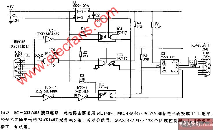
SC-232/485 interface circuit

SC-232/485 interface circuit

FSK modulation and power line interface circuit

FSK modulation and power line interface circuit

High output level RF modulator circuit

High output level RF modulator circuit

USB signal generating circuit diagram


USB signal generating circuit diagram

48V DC input 12V output step-down circuit

nput 12V output step-down circuit

Minimum System Diagram

Minimum system (power supply circuit and I / O expansion and gating circuit) 

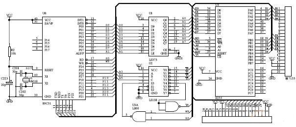
  design uses minimal system board is based on 80C52 microcontroller as the core, and has good scalability. CPU external crystal 11.0592MHz, mainly by 74LS373 latch circuit, 74LS138 decoder circuit and keys, display devices, ICL7135 its peripheral typical circuit, with 8255 foreign expansion of I / O interfaces. Minimum system circuit shown in Figure 2.
2 minimum system schematic diagram
  This circuit requires external transformer an AC220 / 9V, the secondary side of the transformer is rectified and filtered through CW7805 can get + 5V input voltage, this voltage power supply to do the smallest system.
  System by 8255 to expand outside the PA, PB, PC total 24 I / O ports, so that as the system's input and output channels. 74LS138 output as decoded by the selection terminal of each chip, in addition to the minimum outer Y0 ~ Y3 used in the system, as well as Y4 ~ Y7 available to other extensions.

SPI interface with the microcontroller interface schematics (STPM01 and P89LPC94


STPM01 and P89LPC9401 interface design
  STPM01 SPI interface is a two-wire interface, the data input and output pins are the same, with the standard three-wire SPI interface is different. We use the method shown in Figure 3 to connect the two chips.
  As the SPI bus master, LPC9401 output clock signal, STPM01 accordance SCLNLC clock signal for communication. To improve the anti-jamming performance, in series connection in a 10 ~ 100Ω resistor that chip pin input capacitance form a low-pass filter to filter out interference on the connection. When LPC9401 read STPM01 data, use the SPI module chip. And when you write data to STPM01 not use SPI bus control module, and the use of software simulation SPI timing output data. This is designed to consider the meter is running, LPC9401 STPM01 rarely write data to and reading data very frequently. This design takes full advantage of the chip's resources, improve the operating efficiency of the program.
  Sampling circuit design
  Voltage sampling resistor divider, taking into account the limited breakdown voltage chip resistors, the choice of four 200kΩ resistor divider to do. STPM01 maximum voltage channel input differential voltage is ± 0.3V, for 50Hz AC, corresponding valid values ​​0.21VRMS, the input signal can not be larger than this maximum, otherwise there will be clipping. Taking into account the margin for the rated voltage of 220V, we take 0.16VRMS, then
  Sampling resistor = 200 × 4 × 0.16 / 220 = 581Ω, 560Ω we have chosen as the sampling resistor.
  Phase current sensor we use transformers, variable ratio of 5,000: 1. The channel gain is set to 8, the maximum input signal is 0.105VRMS, taking into account a certain margin, in the 40A, the input signal selection around 0.08VRMS, the transformer load resistance of 0.08 / 40 × 5,000 = 10Ω.
  We use the zero line current channel manganin shunt, shunt resistance take 250μΩ.Resistance can not get too big or too small, if the election is too small, the sampling in the small current signal is too weak, causing the error increases, easy-tolerance. If you choose too large, the large current shunt heat is too large, resulting in errors instability.
Figure 3: SPI interface diagram.
  For 250μΩ shunt, the voltage at both ends of the signal 40A is 250 × 40 = 10,000μV, i.e. 10mVRMS. The sampling signal is very small, so the channel should be set to the maximum gain that is 32 times, the maximum amplitude of the signal input at this time is 26.25mVRMS.The actual maximum input signal is less than the maximum allowable input signal, shunt resistance reasonable choice.

The new ultrasound technology enables implantation equipment from radio interference

The new ultrasound technology enables implantation equipment from radio interference
An ultrasonic technology could help prevent heart pacemakers and other implantable medical devices by radio attack.
  A new method of the Swiss Federal Institute of Technology researchers and the French Institute of Computer and Control, National Institute of Development Science is built by using ultrasonic testing of implantable medical devices and radio exact distance. The device requires only a microphone to detect ultrasound, and does not consume too much energy. Since the device does not respond to a predetermined distance beyond the interference, so the power consumed is not endless.
  Researchers have built and tested a prototype system, and has applied for a patent. The study presented at the American Conference on Computer (ACM) Computer and Communications Security (CCS), the Association during the meeting held in November in Chicago (Illinois, USA) in 2009.

Phase Change Memory: The new memory can be realized using a new memory model


Phase Change Memory: The new memory can be realized using a new memory model
Several important features from below, the phase-change memory (PCM) technology are in line with the current needs of electronic systems for the memory subsystem:
Capacity
- because of consumer electronics, computers, communications application trends triple, the amount of code that all electronic systems are growing at a rate of exponential data growth rate is even faster.
Bandwidth and energy consumption
- in the application of highly integrated electronic systems, in order to speed up the Internet speed, using bandwidth to measure system performance; enhancement products for mobile use, the use of power system performance evaluation. Memory must be designed to support the demand for expanded bandwidth and lower power consumption growing. A non-volatile solid-state memory is the best way to reduce power consumption.
Memory system
- in order to improve the overall performance of electronic systems, designers are increasingly concerned about the capacity of the memory system, technical performance, packaging and interface parameters.
Cache
 - "memory system" does not support the concept of classification according to the memory technology, and support the bandwidth requirements of the final device according to memory classification, thus overcoming the memory technically design challenges, by temporarily retain and optimize the combination of different storage technologies to reduce product costs, improve system performance.
Bandwidth classification
from a higher level, we can consider three bandwidth categories: code, data flow and data storage.
Code
- read speed is the major determinant of code execution performance. When using one of the following modes, depending on the execution speed of code execution performance: execution (XIP) chip: the use of NOR flash requires a large bandwidth and random read speed; storage and downloading (S & D): the use of NAND + DRAM memory. S & D is a method of code storage capacity greater than 1Gb widely adopted.
Data streams
- data flows affect the performance of the main factors is the write speed. Stream usually DRAM technology, however, may be greater than the capacity of 4GB NAND + DRAM using a method is mainly used to increase capacity and reduce power consumption.
Data Storage
- affecting data storage performance is a major factor in memory capacity and data retention.However, due to the memory capacity growing at the rate of exponential growth, the delay between the different system components may affect the performance of the memory subsystem constitutes a big impact. 100GB capacity following high demands on performance or data storage commonly use NAND flash memory.
High-density memory technology overview
Figure 1 - high density memory technology overview
PCM upgrade capability
chalcogenide (PCM) application in at least three aspects of the film proved able to upgrade to at least PCM storage unit 5nm node. The main challenge facing the PCM technology upgrade is to upgrade the switch components. Because the state of research and improved control methods chalcogenide thin film materials, PCM-resistant ability to read and write and write speeds are expected in the near future there will be increased dramatically. With the process of the most advanced lithography techniques to enter the node, and write performance cost per PCM great progress is expected, because the storage unit in the nodes of these techniques can be made ​​smaller.
PCM in embedded systems
in embedded systems, PCM is usually used to store data. Storage capacity requirements for lower system capacity is usually less than about 2Gb, designed to execute code directly from the flash memory NOR. In embedded systems, this memory is usually also used to store system files. Such systems typically act as a DRAM process using scratchpad.
In such systems, PCM used for code execution memory because it is a bit-erasable memory, PCM system can replace some of the DRAM needed. 
In the "store and download memory" memory system, PCM can reduce capacity requirements for DRAM, but can also meet the capacity needs of the NAND. Meanwhile, the use of such systems in the PCM memory may be stored in the same memory to simplify the file system, and to improve file system performance.
SnD and XiP system architecture
Figure 2 - SnD and XiP system architecture
PCM in a wireless communication system,
within a very short time delay to read quickly override function, PCM is an ideal non-volatile memory chip code execution solution from the low capacity to apply a variety of high-capacity storage applications. Although PCM read latency than DRAM long, but relatively small memory page read latency DRAM level or belong to, it can serve as a very good code execution memory.In addition to the data structure often operated, PCM can be used as a regular memory read all the data structures. PCM bit can erase function eliminates the need for block erase, while further reducing the demand for DRAM, thereby reducing the cost of the storage subsystem.
PCM is expected to become one of the lowest overall cost scalable memory subsystem solutions, while meeting the growing market demand for high-end multimedia wireless device performance.
PCM can improve the performance of advanced embedded systems, which has been proven in high-end wireless communications system
Click to see image

Figure 3 - PCM can improve the performance of advanced embedded systems, which has been proven in high-end wireless communications system
PCM in the solid state storage subsystem
because of the inherent characteristics of the block can be erased NAND technology, implemented in the solid-state storage subsystem Managing NAND is a big challenge. When a large number of erase operations or frequent read operations, memory error prone, leading to the need for error management mechanism, and error management mechanisms to meet the increasing demands of the market is also a challenge. 
PCM processor can be saved in the solid-state storage systems frequently visited pages, as well as those operating data within the chip when more manageable elements, including NAND save data required parity, bad block table, block page mapping table and so on. In this case, the PCM can improve the manageability of NAND. By minimizing the NAND flash memory by the stress in the storage subsystem can achieve higher-capacity multi-level cell NAND flash memory using NAND PCM to reduce the cost function. This use as a PCM buffer solution will improve the performance and reliability of the storage subsystem.
Hybrid solid state memory
Figure 4 - mixing solid state memory
Further, when the dispersion of the erased pages in the plurality of blocks (nearly filled state), PCM can be further improved reliability of the storage subsystem. Management can block nearly filled state
Erase memory, you need to complete a number of erase cycles before for new data to be written to memory to free up space, and this will increase the endurance of memory, speed up the life of memory, up to a maximum endurance so far.
PCM bit can erase feature can solve the increased number of write cycles when the problem when the memory is full, the higher the number of read and write PCM systems can meet these requirements at the time of overload use.
PCM computer platform
as a volatile memory, DRAM requires a lot of energy stored content (W / GB). As a non-volatile memory, when the content does not need to PCM, PCM module can turn off the power, thereby reducing standby power consumption, more importantly, cut off contact between capacity and power consumption. This creates a capacity limit from PCM memory subsystem power limitation.In addition to the non-volatile external, PCM provides attractive for this application the ability to read and write delay resistance, compared with the current read and write frequently tried solution resistance, and the ability to read and write the write delay is a major advantage of PCM.
Conclusion The
PCM is a sustainable development and devastating memory technology has. From the viewpoint of complementarity, the two properties can accelerate market penetration of the PCM. In addition, PCM can be used for memory systems, and consumer electronics, computer, communications triple applications. This article also discusses some of the PCM storage systems to different penetration problems. Temporarily retain existing memory technologies, reducing overall system cost and system complexity, will be convincing motive recommend using PCM solutions.
In the code and data transmission applications, the bandwidth PCM will promote sustainable development, and low power consumption is another value-added feature of this technology.

PWM motor / lamp controller circuit -PWM Motor / Light C

PWM motor / lamp controller circuit -PWM Motor / Light Controller
A Pulse width Modulator ( PWM ) is a device That May be Used as an Efficient light DIMMER or DC Motor Speed ​​Controller. DESCRIBED The circuit here is a General Purpose DC device That CAN Control Devices Which Draw up to a FEW amps of current. The circuit may be used in 12 Volt and 24 Volt systems with a few minor changes. This device has been used to control the brightness of an automotive tail lamp and as a motor speed control for small DC fans of the type used in computer power supplies. A PWM circuit works by making a square wave with a variable on-to-off ratio, the average on time may be varied from 0 to 100 percent. In this manner, a variable amount of power is transferred to the load. The main advantage of a PWM circuit over a resistive power controller is the efficiency, at a 50% level, the PWM will use about 50% of full power, almost all of which is transferred to the load, a resistive controller at 50% load power would consume about 71% of full power, 50% of the power goes to the load and the other 21% is wasted heating the dropping resistor. Load efficiency is almost always a critical factor in alternative energy systems. An additional advantage of pulse width modulation is that the pulses are at the full supply voltage and will produce more torque in a motor by being able to overcome the internal motor resistances more easily. Finally, in a PWM circuit, common small potentiometers may be used to control a wide variety of loads whereas large and expensive high power variable resistors are needed for resistive controllers. The main Disadvantages of PWM circuits are the added complexity and the possibility of generating radio frequency interference (RFI). RFI may be minimized by locating the controller near the load, using short leads, and in some cases, using additional filtering on the power supply leads. This circuit has some RFI bypassing and produced minimal interference with an AM radio that was located under a foot away. If additional filtering is needed, a car radio line choke may be placed in series with the DC power input, be sure not to exceed the current rating of the choke.
SPECIFICATIONS
PWM Frequency: 400 Hz
Current Capacity: 3 Amps with IRF521 FET, More with IRFZ34N FET
PWM circuit current: 1.5 mA @ 12V with no LED and no load
Operating Voltage: 12V or 24V DEPENDING on the configuration.
THEORY
The PWM circuit Requires a steadily running Oscillator to Operate. U1a and U1d form a Square / Triangle Waveform Generator with a Frequency of around 400 Hz. U1c is Used to generate a 6 Volt Reference current Which is Used as a Virtual Ground for the Oscillator , this is necessary to allow the oscillator to run off of a single supply instead of a +/- voltage dual supply. U1b is wired in a comparator configuration and is the part of the circuit that generates the variable pulse width. U1 pin 6 receives a variable voltage from the R6, VR1, R7 voltage ladder. This is compared to the triangle waveform from U1-14. When the waveform is above the pin 6 voltage, U1 produces a high output. Conversely, when the waveform is below the pin 6 voltage, U1 produces a low output. By varying the pin 6 voltage, the on / off points are moved up and down the triangle wave, producing a variable pulse width. Resistors R6 and R7 are used to set the end points of the VR1 control, the values ​​shown allow the control to have a full on and a full off setting within the travel of the potentiometer. These part values ​​may be varied to change the behavior of the potentiometer. Finally, Q1 is the power switch, it receives the modulated pulse width voltage on the gate terminal and switches the load current on and off through the Source-Drain current path. When Q1 is on, it provides a ground path for the load, when Q1 is off, the load's ground is floating. Care should be taken to insure that the load terminals are not grounded or a short will occur. The load will have the supply voltage on the positive side at all times. LED1 is optional and gives a variable brightness response to the pulse width. Capacitor C3 smooths out the switching waveform and removes some RFI, Diode D1 is a flywheel diode that shorts out the reverse voltage kick from inductive motor loads. In the 24 Volt mode, regulator U2 converts the 24 Volt supply to 12 Volts for running the pwm circuit, Q1 switches the 24 Volt load to ground just like it does for the 12 Volt load. See the schematic for instructions on wiring the circuit for 12 Volts or 24 Volts. At the 1 amp current level, no heat sink is needed on Q1, if you will be switching more current, a heat sink is recommended. Q1 may be replaced with a higher current device such as an IRFZ34N, all of the current handling devices, switch S1, fuse F1, and the wiring between the FET, power supply, and load should be able to handle the maximum load current.
CONSTRUCTON
The prototype for this circuit WAS Constructed on a regular IC proto Board with Parts and wires stuck into the proto Board holes. One Version of the Finished circuit WAS Used to make a variable DC Fan Speed, the Fan WAS mounted on Top of a Small Metal Box and thePWM circuit WAS CONTAINED Inside of the Box (Fig 1). I Built a Simple circuit Board (Fig 2) using a CAD program free circuit Board, PCB (1) That runs on the Linux Operating system. The circuit Board image was printed on a PostScript laser printer onto a mask transfer product called Techniks Press-n-Peel blue film (2). The printed on film is then ironed on to a cleaned piece of single sided copper clad board. The board is etched with Ferric Chloride solution. Holes are drilled with a fine gauge drill bit, parts are soldered in, and the board is wired to the power and load. This technique is great for producing working boards in a short time but is not suitable for large numbers of boards. A board pattern is shown in Fig 3, this may be photo-copied onto a piece of press-n-peel blue film. Alternately, the dead-bug construction method may be used, this involves taking a piece of blank copper PC board, glueing a wire-wrap IC socket to the board with 5 minute epoxy, then soldering all of the parts to the wire wrap pins. Grounded pins can be soldered directly to the copper board.
ALIGNMENT
No Alignment Necessary SHOULD be with this circuit.
PARTS
U1: LM324N Quad op-amp
U2: 78L12 12 volt Regulator
Q1: IRF521 N Channel MosFet
D1: 1N4004 silicon Diode
LED1 Red LED
C1: 0.01uF Ceramic Disc Capacitor, 25V
C2-C5: 0.1uF Ceramic Disk Capacitor, 50V
R1 R4: 100K 1 / 4W resistor
R5: 47K 1 / 4W resistor
R6-R7: 3.9K 1 / 4W resistor
R8: 2.7K 1 / 4W resistor
VR1: 10K linear Potentiometer
F1: 3 Amp, 28V DC fast Blow fuse
S1: Toggle switch, 5 Amps
USE
This circuit Will work as a DC lamp DIMMER, Small Motor Controller, and Even as a Small Heater Controller. It Would make a great Speed ​​Control for a Solar Powered electric Train. I have not Tried the circuit with larger motors, in theory, it should work in applications such as a bicycle motor drive system, if you experiment with this, be sure to include an easily accessible emergency power disconnect switch in case the FET shorts on. Wire the circuit for 12 Volts or 24 Volts as per the schematic , connect the battery to the input terminals, and connect the load to the output terminals, be sure not to ground either output terminal or anything connected to the output terminals such as a motor case. Turn the potentiometer knob back and forth, the load should show variable speed or light.

[Editor: electronic enthusiasts --- reproduced, please indicate the source] 

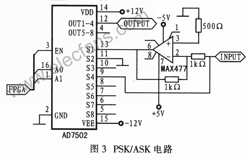
Based FPGA-ASK Circuit SD7502 constituted

SD7502 constitute based FPGA -ASK Circuit
FPGA-ASK circuit

4 outputs obtained from a DA converter decode multi-channel switching circuit


4 outputs obtained from a DA converter decode multi-channel switching circuit
The function of the circuit
When multi-channel analog inputs connected switcher, multi-channel AD converter, such as channel scan speed is relatively slow, mostly with multiple AD conversion circuitry. The circuit on the contrary, is put into a DA converter 4 outputs form four equivalent DA converter, which is used to allow the slow conversion speed DA output circuits, the cost can be reduced.
Circuit works
Work on the principle of the circuit, just think about the DA converter output is terminated with a 4 contact rotary switch, and high-speed rotating shaft, it is easy to understand.
IC2 2-4 decoder which according to the input data "L", "L" is YO; "L", "H" for Y1; "H", "L" for Y2; "H", "H" Y3 for combinations, so that the two data corresponding output Y becomes "L" level, driving four-way analog switch IC.
When the input of IC2 G "H" level, since all Y outputs are "H", this state can be maintained as a signal sampling or. Output order data is as follows:
Assuming the value of the DA converter circuit by double lock, the input to channel 1, first to make A, B for the two-input "L", "L", the switch S1 is closed, the channel 1 is selected.
Next, as a signal input is sampled, the desired pulse width to ensure that the capacitor C1 to be fully charged, the output from the DA in order to zero to + 10V when charging C1 accuracy within 0.1%, the pulse width PW must meet the requirements of the following formulas: PW≥1000C1.R1, R1 = 1K, C2 = 0.01UF, PW = 10MS. Thus, scanning four output channels requires a minimum 40MS.
If you let A = "H", B = "L", the selector switch S2 can make the DA data input to Channel 2.Finally, in order Channel 3, Channel 4, and repeat the process.
The voltage produced when the capacitor is charged, the bias current is high input impedance, low input amplifier OP held until the next sampling cycle. Each output stage offset adjustment circuit is not connected, the offset can be adjusted by the next level of the circuit as needed.
Optional components
Capacitor C1 ~ C4 are holding capacitor voltage, high insulation resistance should be selected product, the choice of film capacitors. And do not pay attention to the capacitor near the power cord. Wired logic circuits should be so, if there is capacitive coupling, because the logic signal is unipolar, so the capacitor will be positive charge, equivalent to happen bias drift. There are four combinations of OP amplifier selection of LT084, if FET input can also choose other types of OP amplifier.
C5 ~ C8 to stabilize the feedback circuit which is not strictly required capacity size.

Interface module circuit

This circuit current limiting effect.
When current flows through the Q5B R33, when the voltage across R3 is greater than 0.7V, Q5A starts conducting, so that the base voltage is increased Q5B prevent Q5B current increases.
Because it is immediate negative feedback circuit, does not produce shocks.

TTL remote communications interface circuits

TTL remote communications interface circuits

DK04 monitoring module and computer communications interface circuits

As shown, D187 is a universal asynchronous receiver transmitter (UART), its RX / TX signal received optocoupler N21, the N22 and N29, so put the RS-485 communication interface receiver / transmitter D28 and micro-processing D211 is completely converted into power for ± l2V communication dedicated RS-232 driver chip

DMAl0 rectifier function chart

DMAl0 rectifier function diagram:

ATMEGA16 microcontroller keyboard and display circuit

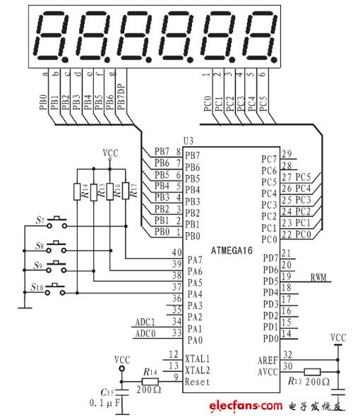
   Input and display circuit using four buttons, and finished with a function to switch the output voltage setting and display switching. Show some use common anode digital tube dynamic display, as shown. MCU ATMEGA16using the internal 8 MHz crystal.
  
ATMEGA16 microcontroller keyboard and display circuit

  Figure keyboard and display circuit

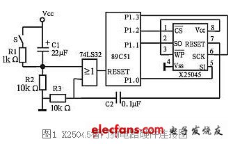
89C51 microcontroller + watchdog circuit composed X25045

   Using 89C51 microcontroller and X25045 composed watchdog circuit , X25045 hardware connection diagram shown in Figure 1. The X25045 chip contains a watchdog timer can be preset by the system software to monitor the time. In the watchdog timer preset time if there is no bus activity, the X25045 will RESET outputs a high level signal, through differential circuit C2, R3 outputs a positive pulse, the CPU is reset.The circuit of Figure 1, the reset signal to the CPU of a total 3: Power-on reset (C1, R2), manual reset (S, R1, R2) and Watchdog Reset (C2, R3), added after the adoption of a comprehensive RESET terminal or gate. C2, R3 do not have a time constant is too large, there can be hundreds of microseconds, because then the CPU oscillator already working.
  
89C51 microcontroller + watchdog circuit composed X25045

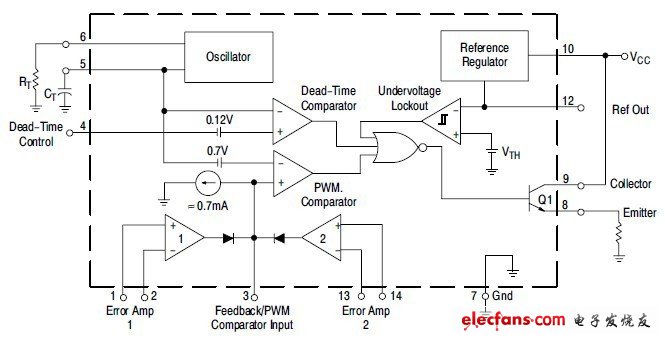
MC33060 circuit diagram of the internal structure

MC33060 is a performance by ON (ON Semi) semiconductor company produces excellent pulse-width modulated voltage-driven devices, the use of fixed-frequency single-ended output, can work in -40 ℃ to 85 ℃. Its internal structure shown in Figure 1 [1], the main features are as follows:
  1) all of the pulse width modulator integrated circuit;
  2) Built-linear sawtooth oscillator, external components only one resistor capacitor;
  3) Built-in error amplifier;
  4) Built-in 5V reference voltage, 1.5% accuracy;
  5) Adjustable dead zone control;
  6) Built-in 200mA drive capability of the transistor provided;
  7) undervoltage lockout protection;


  Internal Structure Figure 1 MC33060

MCU multiplication circuit

MCU multiplication circuit can be fed in different X and Y inputs, or using a simple single-ended input. Connect the input determines the polarity of the output.
MCU multiplication circuit

TPS92310 typical application circuit and topology

This article describes the main characteristics of the circuit diagram TPS92310, a block diagram of a typical application circuit, isolated and non-isolated topologies
  
TPS92310 block diagram

  Block diagram of Figure 1.TPS92310
  
A typical application circuit TPS92310

  Typical application circuit diagram 2.TPS92310
  
TPS92310 isolated topologies Circuit

  Topology Diagram Figure 3.TPS92310 isolation
  
TPS92310 non-isolated topologies Circuit

  Figure 4.TPS92310 non-isolated topologies Circuit

uP constitute a watchdog circuit monitors

MAX706's internal watchdog timer timing of 1.6 seconds, if within 1.6 seconds, the watchdog input pin WDI maintained at a predetermined level (high or low), the watchdog output Duanli goes low, diode D is turned on, so that a low level is applied to the reset terminal, MAX706 generates a reset signal RESET reset the device until it is cleared after reset watchdog, Li only goes high. When WDI has an edge (rising or falling) signal, the watchdog timer is cleared.

uP constitute a watchdog circuit monitors

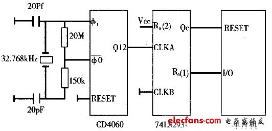
TTL-type watchdog circuit

By CD4060 and 32.768Hz composed of quartz oscillator pulse generating circuit generates 4Hz pulse source. 74LS293 counter 4Hz pulse source is counted, its output Q is connected to the microcontroller reset terminal RESET, certain I / O terminal is connected to the microcontroller 74LS293's clear terminal R, the program within 1.5 seconds of the first output from low to high and because of narrow pulses from high to low, the output Q has been low, otherwise the output is high .TTL type watchdog circuit :

TTL-type watchdog circuit

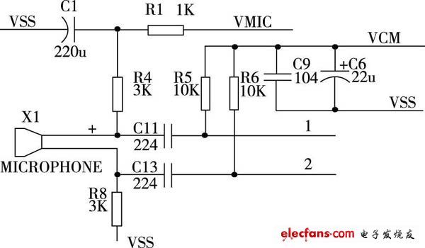
Smart Car voice input circuit

Smart Car voice input circuit as shown. Among them, VM IC provides power to the microphone, VSS is the system's analog ground, VCM is the reference voltage, a foot and two feet respectively microphone X1 is positive, the negative input pin. When speaking in front of the microphone when a foot and two feet will produce along with voice microphone input waveform change and the formation of two inverted waveform at SPCE061A at two ports, and sent SPCE061A controller internal operational amplifier Audio amplification, the amplified audio signal converted by the ADC to digital converter, stored in the corresponding register, and then compresses the digital audio signal, identification, playback processing.
  
Smart Car voice input circuit

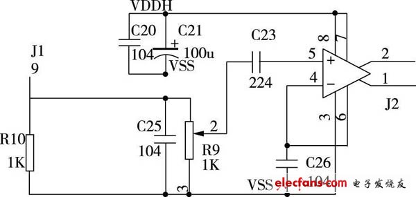
Smart car speech output circuit

Smart car speech output circuit as shown.Wherein, VDDH reference voltage, VSS is the system's analog ground. The audio signal to the DAC by SPCE061A output circuit 9 pin end, by adjusting the volume potentiometer R9 end integrated audio amplifier sent SPY0030, amplified by the audio, the audio signal is output from SPY0030 J2 port via an external speaker to play sounds.
  
Smart car speech output circuit

Smart car driver circuit

Smart car driver circuit is a full bridge driver circuit, Q1, Q2, Q3, Q4 transistor consisting of four four-arm, Q5 control Q2 and Q3 is turned on and off, Q6 control Q1 and Q4 are turned on and off , the driving circuit for the rear wheels, respectively the front direction of the driving circuit and the driving circuit. When a pin is high, 2 pin low conduction always Q1 and Q4, Q2, and Q3 is turned off, the motor drives the wheels running; When a pin is low, the two pin is high time to time As of Q1 and Q4, Q2, and Q3 is turned on, the motor drives the wheels reverse direction.
  
Smart car driver circuit

Basketball timing and scoring system diagram

 Keyboard a bit more, used on six, two and even a separate keyboard interrupt port, four matrix keyboard is used to adjust the score.

Serial Communications schematic and PCB diagram between SCM and computer

Figure 1 Schematic microcontroller serial communications between computers


PCB diagram in Figure 2 serial communication between the microcontroller and the computer

Hardware timer circuit diagram answer and vote


The schematic from the paper, "Design and Implementation of Intelligent timer AT89C51 answer and vote based on"  

AT89S51 microcontroller-based timing alarm circuit diagram

Design a simple timer alarm microprocessor controlled. Requirements according to the initial value set (1-59 seconds) countdown timer to 0:00 when digital tube flashes "00" (at 1Hz flashing), the key features are as follows:
  (A) setting key: When the countdown mode, press this button to stop the countdown after enter setting mode; If you have already set up a state in this key is invalid. (2) by a key: When setting the state, each time the increment key figures of the initial value by one. (3) delivery of a key: When setting state, decreasing each time the key figures of the initial value minus 1. (4) Enter key: After setting state, press this button, SCM initial value under the new countdown and display digital countdown. If the state is already in the timing of this key is invalid.

Figure timing alarm circuit schematics

DDS signal source circuit diagram based on the AVR microcontroller

Circuit schematic shown below, can be divided into four parts: the IC1 as the core of DDS; to IC2 as the core of a keyboard, display and control circuit; to IC3 as the core of AGC circuit; IC4 as the core to the detector circuit.
Figure DDS signal source circuit diagram based on AVR microcontroller

DM9000A peripheral circuit


The schematic diagram details, see the following links

Serial communication experiment circuit diagram AT89 series microcontrollers and PC

AT89 series microcontrollers and PC serial communication experiment Circuit:

Move around the circuit diagram microcontroller based advertising lights

Single lights left to do right, the hardware circuit as shown, eight light-emitting diode L1 - L8 were connected to the MCU P1.0 - P1.7 interface on when the output "0", the LED lights, at the beginning P1.0 → P1.1 → P1.2 → P1.3 → ┅ → P1.7 → P1.6 → ┅ → P1.0 bright, repeat the cycle.
  The "SCM system" area of ​​P1.0 - P1.7 with 8-core cable connected to the "Eight LEDs indicate module" area of ​​L1 - L8 on the port requirements: P1.0 corresponds to L1, P1.1 corresponding to the L2, ... ... P1.7 corresponds L8.

Move around a circuit diagram of microcontroller-based advertising lights

Multiplexer-based C51 MCU status display circuit schematics

shown below, AT89S51 MCU P1.0 - P1.3 pick four light-emitting diodes L1 - L4, P1.4 - P1.7 pick up four switches K1 - K4, programming will reflect the state of the switch to the light-emitting diodes . (The switch is closed, the corresponding lights, switch off, the corresponding light off).
1. The "SCM system" area of P1.0 - P1.3 with a wire connected to the "Eight LEDs indicate module" area of L1 - L4 port;
2. The "SCM system" area of P1.4 - P1.7 with a wire connected to the "four toggle switch" area of K1 - K4 port.

Alarm generator circuit schematic-based C51 MCU

1KHz and 500Hz with P1.0 output audio signal to drive the speaker, as an alarm signal, requiring 1KH z signal loud 100ms, 500Hz signal loud 200ms, alternately, P1.7 connect a switch to control when the switch is closed loud alarm signal, When the switch is turned off warning signals to stop, to compile the program.
  (1 of the "SCM system" area of ​​P1.0 port with a wire connected to the "Audio amplifier module" area of ​​SPK IN port;
  (2 in the "Audio amplifier module" area on the SPK OUT port connected to either 16 ohm speaker an 8 ohm;
  (3 of the "SCM system" area P1.7 / RD port with a wire connected to the "four toggle switch" area K1 port.